PDF

Power Transistor
Introduction
Transistors are building blocks of electronic appliances, and can be found in radios, computers, and calculators, to name a few. When working with electrical systems you typically have to deal with heat transfer; electric heating is often an unwanted result of current conduction.
This example simulates a system consisting of a small part of a circuit board containing a power transistor and the copper pathways connected to the transistor. The purpose of the simulation is to estimate the operating temperature of the transistor, which can be substantially higher than room temperature due to undesired electric heating.
Transistors are semiconductor devices used to switch or amplify electronic signals. There are different types of transistors, ranging in size depending on how they are packaged. Power transistors carry and dissipate more power and therefore come in larger packages. These packages can be attached to a heat sink for better cooling and to avoid overheating of the system.
The heat sink would then be attached to the transistor via the copper plate located behind the ceramic piece (shown in Figure 1 to the left). While it’s often important to construct a way to cool electronic systems, such as in the case of components in hybrid cars, each system has its own acceptable operating temperature range. What determines the maximum and minimum temperature limits include the semiconductor material properties, the transistor type, the design of the device, and so forth. There is a conventional temperature range, however, which is thought to be between -55 °C and 125 °C.
Model Definition
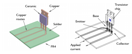
Figure 1 shows the model geometry used in the simulation. The power transistor is mounted on the circuit board using through-hole technology. The solder in the holes give mechanical support and electronic contact between the copper routes and the transistor pins.
Figure 1: Model geometry and position of transistor chip.
The transistor chip itself is a very thin structure represented by an internal surface in Figure 1. The chip is connected to the pins but this connections are assumed to have negligible effects on heat transfer.
The transistor package front part is made of ceramics while the back part, which could be clamped to a heat sink, is made of copper. The transistor chip and the front part of the package have matching thermal properties. The copper pins are soldered to the circuit board by the solder material 60Sn-40Pb (60 % tin and 40 % lead). The circuit board is made of FR4.
Current conduction and Joule heating take place in the copper routes, in the solders, and in the pins. In these parts, the physics of heat transfer and heat production due to Joule heating are fully coupled to the conduction of electric current. In all other parts of the transistor, only heat transfer and heat production take place.
The transistor chip itself is represented by an internal boundary with an internal production of heat corresponding to 0.9 W. Cooling through convection takes place at all external boundaries with a heat transfer coefficient of 5.0 W/(m2·K). This value of the heat transfer coefficient corresponds to the worst case scenario when the fan is switched off. The ambient temperature is 293.15 K.
Current enters the circuit board at the left vertical boundaries of the copper routes connected to the base, emitter, and collector in Figure 1. The value of the current at the boundary of the route connected to the emitter is 0.12 A. The value of the current at the boundary of the route connected to the collector is 0.11988 A. The difference in absolute current between the emitter and collector currents corresponds to the current at the boundary of the route connected to the base, which is 0.12 mA.
Results and Discussion
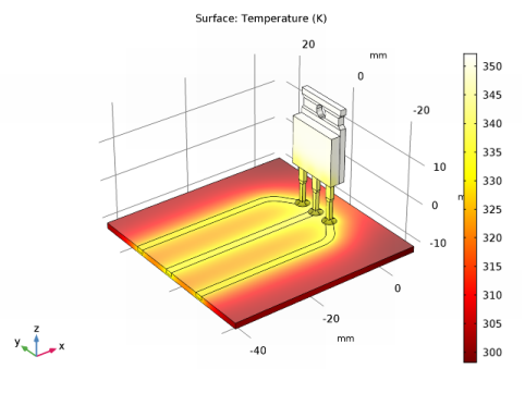
Figure 2 below shows the temperature distribution in the device. The maximum temperature is about 354 K or 81 °C. This is well within the acceptable operation temperature range for the transistor, which implies that attaching it to a heat sink is not needed in this case.
Figure 2: Temperature distribution.
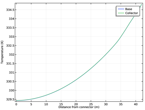
Also worth noting is that electric heating, or Joule heating as it is also referred to, hardly influences the temperature of the copper routes at the distance from the transistor modeled above. That’s most likely due to copper’s high conductivity; some of the heat produced in the transistor chip is conducted away from the device via the copper routes. Figure 3 shows the temperature along the copper routes connected to the base and the collector respectively. The current density in the base is 1/1000 of that in the collector but the temperature in the copper routes connected to the base and collector is almost identical.
Figure 3: Temperature along the copper routes connected to the base and collector.
The fact that the Joule heating effect does not increase temperature in the copper routes leads to the conclusion that the higher temperature in these routes is due to coppers high conductivity. The copper routes conduct some of the heat produced in the transistor chip away from this device. The circuit board has a poor thermal conductivity and is therefore not heated to the same extent as the copper routes.
Notes About the COMSOL Implementation
You can find all the material properties for this application in COMSOL’s Material Library. Furthermore, the ready-made physics interface for Joule heating sets up all model formulations that you need for the simulation: Electric Current and Heat Transfer in Solids are added with the corresponding Joule Heating coupling features in the Multiphysics node.
The Joule heating interface is by default available for all materials in the model. However, the circuit board material and the package material do no conduct electric current. For this reason, you have to edit the selection of Electric current physics to remove non-conducting domains. On the circuit board material, only heat transfer physics is calculated. By removing the non-conductive parts of the device to the list of Electric Current physics, Electromagnetic Heat Source and Boundary Electromagnetic Heat Source are automatically not applicable on these domains.
Application Library path: Heat_Transfer_Module/Power_Electronics_and_Electronic_Cooling/power_transistor
Modeling Instructions
From the File menu, choose New.
New
In the New window, click Model Wizard.
Model Wizard
1
In the Model Wizard window, click 3D.
2
In the Select Physics tree, select Heat Transfer>Electromagnetic Heating>Joule Heating.
3
Click Add.
4
Click Study.
5
In the Select Study tree, select Preset Studies for Selected Physics Interfaces>Stationary.
6
Click Done.
Geometry 1
The geometry sequence for the model is available in a file. If you want to create it from scratch yourself, you can follow the instructions in the Geometry Modeling Instructions section. Otherwise, insert the geometry sequence as follows:
1
On the Geometry toolbar, click Insert Sequence.
2
3
On the Geometry toolbar, click Build All.
4
Click the Zoom Extents button on the Graphics toolbar.
You should now see the geometry shown above.
Global Definitions
Parameters
1
On the Home toolbar, click Parameters.
2
In the Settings window for Parameters, locate the Parameters section.
3
Add Material
1
On the Home toolbar, click Add Material to open the Add Material window.
2
Go to the Add Material window.
3
In the tree, select Built-In>Copper.
4
Click Add to Component in the window toolbar.
Add Material
1
Go to the Add Material window.
2
In the tree, select Built-In>FR4 (Circuit Board).
3
Click Add to Component in the window toolbar.
Add Material
1
Go to the Add Material window.
2
In the tree, select Built-In>Silica glass.
3
Click Add to Component in the window toolbar.
Add Material
1
Go to the Add Material window.
2
In the tree, select Built-In>Solder, 60Sn-40Pb.
3
Click Add to Component in the window toolbar.
Materials
Solder, 60Sn-40Pb (mat4)
On the Home toolbar, click Add Material to close the Add Material window.
Copper (mat1)
1
Click the Wireframe Rendering button on the Graphics toolbar.
2
In the Model Builder window, under Component 1 (comp1)>Materials click Copper (mat1).
3
In the Settings window for Material, locate the Geometric Entity Selection section.
4
Click Clear Selection.
5
FR4 (Circuit Board) (mat2)
1
In the Model Builder window, under Component 1 (comp1)>Materials click FR4 (Circuit Board) (mat2).
2
Silica glass (mat3)
1
In the Model Builder window, under Component 1 (comp1)>Materials click Silica glass (mat3).
2
Solder, 60Sn-40Pb (mat4)
1
In the Model Builder window, under Component 1 (comp1)>Materials click Solder, 60Sn-40Pb (mat4).
2
3
In the Settings window for Material, locate the Material Contents section.
4
Electric Currents (ec)
1
In the Model Builder window, under Component 1 (comp1) click Electric Currents (ec).
2
Ground 1
1
On the Physics toolbar, click Boundaries and choose Ground.
2
Normal Current Density 1
1
On the Physics toolbar, click Boundaries and choose Normal Current Density.
2
3
In the Settings window for Normal Current Density, locate the Normal Current Density section.
4
In the Jn text field, type (1-1e-3)*j_CE.
Normal Current Density 2
1
On the Physics toolbar, click Boundaries and choose Normal Current Density.
2
3
In the Settings window for Normal Current Density, locate the Normal Current Density section.
4
In the Jn text field, type -j_CE.
Normal Current Density 3
1
On the Physics toolbar, click Boundaries and choose Normal Current Density.
2
3
In the Settings window for Normal Current Density, locate the Normal Current Density section.
4
In the Jn text field, type 1e-3*j_CE.
Heat Transfer in Solids (ht)
In the Model Builder window, under Component 1 (comp1) click Heat Transfer in Solids (ht).
Heat Flux 1
1
On the Physics toolbar, click Boundaries and choose Heat Flux.
2
In the Settings window for Heat Flux, locate the Boundary Selection section.
3
From the Selection list, choose All boundaries.
4
Locate the Heat Flux section. Click the Convective heat flux button.
5
In the h text field, type h_coeff.
Boundary Heat Source 1
1
On the Physics toolbar, click Boundaries and choose Boundary Heat Source.
2
In the Settings window for Boundary Heat Source, locate the Boundary Selection section.
3
From the Selection list, choose Transistor Chip.
4
Locate the Boundary Heat Source section. In the Qb text field, type Q_h.
Mesh 1
1
In the Model Builder window, under Component 1 (comp1) click Mesh 1.
2
In the Settings window for Mesh, locate the Mesh Settings section.
3
From the Element size list, choose Fine.
4
Click Build All.
Study 1
On the Home toolbar, click Compute.
Results
Multislice 1
In the Model Builder window, expand the Electric Potential (ec) node.
Electric Potential (ec)
1
Right-click Multislice 1 and choose Delete.
2
On the Electric Potential (ec) toolbar, click Surface.
Surface 1
1
In the Model Builder window, under Results>Electric Potential (ec) click Surface 1.
2
Click Plot.
Temperature (ht)
The second default plot shows the temperature. Add an arrow plot of the total heat flux.
1
In the Model Builder window, under Results click Temperature (ht).
2
On the Temperature (ht) toolbar, click Arrow Surface.
Arrow Surface 1
1
In the Model Builder window, under Results>Temperature (ht) click Arrow Surface 1.
2
In the Settings window for Arrow Surface, click Replace Expression in the upper-right corner of the Expression section. From the menu, choose Component 1>Heat Transfer in Solids>Domain fluxes>ht.tfluxx,...,ht.tfluxz - Total heat flux.
3
Locate the Coloring and Style section. In the Number of arrows text field, type 5e3.
4
From the Color list, choose Black.
5
On the Temperature (ht) toolbar, click Plot.
6
Click the Zoom In button on the Graphics toolbar.
7
Click the Zoom Extents button on the Graphics toolbar.
Finally, reproduce the plot in Figure 3 by following the steps outlined below.
1D Plot Group 4
1
On the Home toolbar, click Add Plot Group and choose 1D Plot Group.
2
In the Settings window for 1D Plot Group, type Temperature along Copper Routes in the Label text field.
3
On the Temperature along Copper Routes toolbar, click Line Graph.
Line Graph 1
1
In the Model Builder window, under Results>Temperature along Copper Routes click Line Graph 1.
2
3
In the Settings window for Line Graph, click Replace Expression in the upper-right corner of the y-axis data section. From the menu, choose Component 1>Heat Transfer in Solids>Temperature>T - Temperature.
4
Click to expand the Legends section. Select the Show legends check box.
5
From the Legends list, choose Manual.
6
7
On the Temperature along Copper Routes toolbar, click Plot.
Line Graph 2
1
Right-click Results>Temperature along Copper Routes>Line Graph 1 and choose Duplicate.
2
In the Settings window for Line Graph, locate the Selection section.
3
Select the Active toggle button.
4
5
Locate the Legends section. In the table, enter the following settings:
6
On the Temperature along Copper Routes toolbar, click Plot.
Temperature along Copper Routes
1
In the Model Builder window, under Results click Temperature along Copper Routes.
2
In the Settings window for 1D Plot Group, click to expand the Title section.
3
From the Title type list, choose None.
4
Locate the Plot Settings section. Select the x-axis label check box.
5
In the associated text field, type Distance from connector (m).
6
On the Temperature along Copper Routes toolbar, click Plot.
Geometry Modeling Instructions
If you wish to create the geometry yourself, follow these steps.
Geometry 1
1
In the Model Builder window, under Component 1 (comp1) click Geometry 1.
2
In the Settings window for Geometry, locate the Units section.
3
From the Length unit list, choose mm.
Block 1 (blk1)
1
On the Geometry toolbar, click Block.
2
In the Settings window for Block, locate the Size and Shape section.
3
In the Width text field, type 50.
4
In the Depth text field, type 50.
5
In the Height text field, type 1.5.
6
Locate the Position section. In the x text field, type -44.
7
In the y text field, type -25.
8
In the z text field, type -12.
Work Plane 1 (wp1)
1
On the Geometry toolbar, click Work Plane.
2
In the Settings window for Work Plane, locate the Plane Definition section.
3
In the z-coordinate text field, type -10.5.
Plane Geometry
In the Model Builder window, under Component 1 (comp1)>Geometry 1>Work Plane 1 (wp1) click Plane Geometry.
Rectangle 1 (r1)
1
On the Work Plane toolbar, click Primitives and choose Rectangle.
2
In the Settings window for Rectangle, locate the Size and Shape section.
3
In the Width text field, type 34.
4
In the Height text field, type 2.
5
Locate the Position section. In the xw text field, type -44.
6
In the yw text field, type 10.5.
Circle 1 (c1)
1
On the Work Plane toolbar, click Primitives and choose Circle.
2
In the Settings window for Circle, locate the Size and Shape section.
3
In the Sector angle text field, type 180.
4
In the Radius text field, type 6.5.
5
Locate the Position section. In the xw text field, type -10.
6
In the yw text field, type 6.
7
Locate the Rotation Angle section. In the Rotation text field, type -45.
8
Click to expand the Layers section. In the table, enter the following settings:
Circle 2 (c2)
1
On the Work Plane toolbar, click Primitives and choose Circle.
2
In the Settings window for Circle, locate the Size and Shape section.
3
In the Radius text field, type 1.75.
4
Locate the Position section. In the xw text field, type -2.5.
5
In the yw text field, type 5.
6
Locate the Layers section. In the table, enter the following settings:
Tangent 1 (tan1)
1
On the Work Plane toolbar, click Tangent.
2
On the object c1, select Boundary 9 only.
3
In the Settings window for Tangent, locate the Tangent section.
4
Find the Second edge to tangent subsection. Select the Active toggle button.
5
On the object c2, select Boundary 11 only.
6
Tangent 2 (tan2)
1
On the Work Plane toolbar, click Tangent.
2
On the object c1, select Boundary 8 only.
3
In the Settings window for Tangent, locate the Tangent section.
4
Find the Second edge to tangent subsection. Select the Active toggle button.
5
On the object c2, select Boundary 7 only.
6
Convert to Curve 1 (ccur1)
1
On the Work Plane toolbar, click Conversions and choose Convert to Curve.
2
Click in the Graphics window and then press Ctrl+A to select all objects.
3
In the Settings window for Convert to Curve, click Build Selected.
4
On the Work Plane toolbar, click Delete.
Delete Entities 1 (del1)
1
In the Model Builder window, under Component 1 (comp1)>Geometry 1>Work Plane 1 (wp1)>Plane Geometry click Delete Entities 1 (del1).
2
In the Settings window for Delete Entities, locate the Entities or Objects to Delete section.
3
From the Geometric entity level list, choose Boundary.
4
On the object ccur1, select Boundaries 5, 7, 8, 10, 27, 30, and 32 only.
Convert to Solid 1 (csol1)
1
On the Work Plane toolbar, click Conversions and choose Convert to Solid.
2
Union 1 (uni1)
1
On the Work Plane toolbar, click Booleans and Partitions and choose Union.
2
3
In the Settings window for Union, locate the Union section.
4
Clear the Keep interior boundaries check box.
Work Plane 1 (wp1)
In the Model Builder window, under Component 1 (comp1)>Geometry 1 click Work Plane 1 (wp1).
Plane Geometry
1
In the Model Builder window, collapse the Component 1 (comp1)>Geometry 1>Work Plane 1 (wp1)>Plane Geometry node.
2
In the Model Builder window, click Plane Geometry.
Rectangle 2 (r2)
1
On the Work Plane toolbar, click Primitives and choose Rectangle.
2
In the Settings window for Rectangle, locate the Size and Shape section.
3
In the Width text field, type 40.5.
4
In the Height text field, type 2.
5
Locate the Position section. In the xw text field, type -44.
6
In the yw text field, type -1.
Work Plane 1 (wp1)
In the Model Builder window, under Component 1 (comp1)>Geometry 1 click Work Plane 1 (wp1).
Plane Geometry
In the Model Builder window, under Component 1 (comp1)>Geometry 1>Work Plane 1 (wp1) click Plane Geometry.
Circle 3 (c3)
1
On the Work Plane toolbar, click Primitives and choose Circle.
2
In the Settings window for Circle, locate the Size and Shape section.
3
In the Radius text field, type 1.75.
4
Locate the Position section. In the xw text field, type -2.5.
Union 2 (uni2)
1
On the Work Plane toolbar, click Booleans and Partitions and choose Union.
2
Select the objects r2 and c3 only.
3
In the Settings window for Union, locate the Union section.
4
Clear the Keep interior boundaries check box.
Mirror 1 (mir1)
1
On the Work Plane toolbar, click Transforms and choose Mirror.
2
3
In the Settings window for Mirror, locate the Input section.
4
Select the Keep input objects check box.
5
Locate the Normal Vector to Line of Reflection section. In the xw text field, type 0.
6
In the yw text field, type 1.
Work Plane 1 (wp1)
In the Model Builder window, under Component 1 (comp1)>Geometry 1 click Work Plane 1 (wp1).
Extrude 1 (ext1)
1
On the Geometry toolbar, click Extrude.
2
In the Settings window for Extrude, locate the Distances section.
3
Select the Reverse direction check box.
Block 2 (blk2)
1
On the Geometry toolbar, click Block.
2
In the Settings window for Block, locate the Size and Shape section.
3
In the Height text field, type 9.
4
Locate the Position section. In the x text field, type -3.
5
In the y text field, type 4.5.
6
In the z text field, type -14.05.
Block 3 (blk3)
1
On the Geometry toolbar, click Block.
2
In the Settings window for Block, locate the Size and Shape section.
3
In the Depth text field, type 1.75.
4
In the Height text field, type 6.
5
Locate the Position section. In the x text field, type -3.
6
In the y text field, type 4.125.
7
In the z text field, type -4.25.
Hexahedron 1 (hex1)
1
On the Geometry toolbar, click More Primitives and choose Hexahedron.
2
In the Settings window for Hexahedron, locate the Vertices section.
3
In row 1, set x to -3.
4
In row 1, set y to 4.5.
5
In row 1, set z to -5.05.
6
In row 2, set z to -5.05.
7
In row 3, set z to -5.05.
8
In row 4, set z to -5.05.
9
In row 5, set z to -4.25.
10
In row 6, set z to -4.25.
11
In row 7, set z to -4.25.
12
In row 8, set z to -4.25.
13
In row 2, set y to 4.5.
14
In row 3, set y to 5.5.
15
In row 4, set y to 5.5.
16
In row 5, set y to 4.125.
17
In row 6, set y to 4.125.
18
In row 7, set y to 5.875.
19
In row 8, set y to 5.875.
20
In row 2, set x to -2.
21
In row 3, set x to -2.
22
In row 4, set x to -3.
23
In row 5, set x to -3.
24
In row 6, set x to -2.
25
In row 7, set x to -2.
26
In row 8, set x to -3.
Union 1 (uni1)
1
On the Geometry toolbar, click Booleans and Partitions and choose Union.
2
Select the objects blk2, blk3, and hex1 only.
3
In the Settings window for Union, locate the Union section.
4
Clear the Keep interior boundaries check box.
Block 4 (blk4)
1
On the Geometry toolbar, click Block.
2
In the Settings window for Block, locate the Size and Shape section.
3
In the Width text field, type 2.5.
4
In the Depth text field, type 14.
5
In the Height text field, type 12.5.
6
Locate the Position section. In the x text field, type -4.
7
In the y text field, type -7.
Block 5 (blk5)
1
On the Geometry toolbar, click Block.
2
In the Settings window for Block, locate the Size and Shape section.
3
In the Width text field, type 1.5.
4
In the Depth text field, type 14.
5
In the Height text field, type 14.
6
Locate the Position section. In the x text field, type -1.5.
7
In the y text field, type -7.
Block 6 (blk6)
1
On the Geometry toolbar, click Block.
2
In the Settings window for Block, locate the Size and Shape section.
3
In the Width text field, type 1.5.
4
In the Depth text field, type 12.5.
5
In the Height text field, type 2.
6
Locate the Position section. In the x text field, type -1.5.
7
In the y text field, type -6.25.
8
In the z text field, type 14.75.
Block 7 (blk7)
1
On the Geometry toolbar, click Block.
2
In the Settings window for Block, locate the Size and Shape section.
3
In the Width text field, type 1.5.
4
In the Depth text field, type 14.
5
In the Height text field, type 1.5.
6
Locate the Position section. In the x text field, type -1.5.
7
In the y text field, type -7.
8
In the z text field, type 17.5.
Hexahedron 2 (hex2)
1
On the Geometry toolbar, click More Primitives and choose Hexahedron.
2
In the Settings window for Hexahedron, locate the Vertices section.
3
In row 1, set x to -1.5.
4
In row 1, set y to -7.
5
In row 1, set z to 14.
6
In row 2, set y to -7.
7
In row 2, set z to 14.
8
In row 3, set y to 7.
9
In row 3, set z to 14.
10
In row 3, set x to 0.
11
In row 4, set x to -1.5.
12
In row 4, set y to 7.
13
In row 4, set z to 14.
14
In row 5, set x to -1.5.
15
In row 5, set y to -6.25.
16
In row 5, set z to 14.75.
17
In row 6, set y to -6.25.
18
In row 6, set z to 14.75.
19
In row 7, set x to 0.
20
In row 7, set y to 6.25.
21
In row 7, set z to 14.75.
22
In row 8, set x to -1.5.
23
In row 8, set y to 6.25.
24
In row 8, set z to 14.75.
Mirror 1 (mir1)
1
On the Geometry toolbar, click Transforms and choose Mirror.
2
3
In the Settings window for Mirror, locate the Input section.
4
Select the Keep input objects check box.
5
Locate the Point on Plane of Reflection section. In the z text field, type 15.75.
Union 2 (uni2)
1
On the Geometry toolbar, click Booleans and Partitions and choose Union.
2
Select the objects hex2, blk7, blk6, blk5, and mir1 only.
3
In the Settings window for Union, locate the Union section.
4
Clear the Keep interior boundaries check box.
Cylinder 1 (cyl1)
1
On the Geometry toolbar, click Cylinder.
2
In the Settings window for Cylinder, locate the Size and Shape section.
3
In the Radius text field, type 1.65.
4
In the Height text field, type 1.5.
5
Locate the Position section. In the x text field, type -1.5.
6
In the z text field, type 15.75.
7
Locate the Axis section. From the Axis type list, choose x-axis.
Difference 1 (dif1)
1
On the Geometry toolbar, click Booleans and Partitions and choose Difference.
2
3
In the Settings window for Difference, locate the Difference section.
4
Find the Objects to subtract subsection. Select the Active toggle button.
5
Work Plane 2 (wp2)
1
On the Geometry toolbar, click Work Plane.
2
In the Settings window for Work Plane, type Transistor Chip in the Label text field.
3
Locate the Plane Definition section. From the Plane type list, choose Face parallel.
4
On the object dif1, select Boundary 1 only.
Plane Geometry
In the Model Builder window, under Component 1 (comp1)>Geometry 1>Transistor Chip (wp2) click Plane Geometry.
Square 1 (sq1)
1
On the Work Plane toolbar, click Primitives and choose Square.
2
In the Settings window for Square, locate the Size section.
3
In the Side length text field, type 3.
4
Locate the Position section. In the xw text field, type -1.5.
Transistor Chip (wp2)
1
In the Model Builder window, under Component 1 (comp1)>Geometry 1 click Transistor Chip (wp2).
2
In the Settings window for Work Plane, locate the Selections of Resulting Entities section.
3
Select the Resulting objects selection check box.
Work Plane 3 (wp3)
1
On the Geometry toolbar, click Work Plane.
2
In the Settings window for Work Plane, locate the Plane Definition section.
3
From the Plane list, choose yz-plane.
4
In the x-coordinate text field, type -2.5.
Plane Geometry
In the Model Builder window, under Component 1 (comp1)>Geometry 1>Work Plane 3 (wp3) click Plane Geometry.
Rectangle 1 (r1)
1
On the Work Plane toolbar, click Primitives and choose Rectangle.
2
In the Settings window for Rectangle, locate the Size and Shape section.
3
In the Width text field, type 0.4.
4
In the Height text field, type 1.5.
5
Locate the Position section. In the xw text field, type 5.5.
6
In the yw text field, type -12.
Bézier Polygon 1 (b1)
1
On the Work Plane toolbar, click Primitives and choose Bézier Polygon.
2
In the Settings window for Bézier Polygon, locate the Polygon Segments section.
3
Find the Added segments subsection. Click Add Linear.
4
Find the Control points subsection. In row 1, set xw to 5.5.
5
In row 1, set yw to -9.7.
6
In row 2, set xw to 5.5.
7
In row 2, set yw to -10.5.
8
Find the Added segments subsection. Click Add Linear.
9
Find the Control points subsection. In row 2, set xw to 6.75.
10
Find the Added segments subsection. Click Add Quadratic.
11
Find the Control points subsection. In row 2, set xw to 5.5.
12
In row 2, set yw to -10.3.
13
In row 3, set xw to 5.5.
14
In row 3, set yw to -9.7.
15
Find the Weights subsection. In the 2 text field, type 0.5/sqrt(2).
Union 1 (uni1)
1
On the Work Plane toolbar, click Booleans and Partitions and choose Union.
2
Click in the Graphics window and then press Ctrl+A to select both objects.
3
In the Settings window for Union, locate the Union section.
4
Clear the Keep interior boundaries check box.
Work Plane 3 (wp3)
In the Model Builder window, under Component 1 (comp1)>Geometry 1 click Work Plane 3 (wp3).
Revolve 1 (rev1)
1
On the Geometry toolbar, click Revolve.
2
In the Settings window for Revolve, locate the Revolution Angles section.
3
Clear the Keep original faces check box.
4
Locate the Revolution Axis section. From the Axis type list, choose 3D.
5
Find the Point on the revolution axis subsection. In the xw text field, type -2.5.
6
In the yw text field, type 5.
7
In the zw text field, type -5.05.
8
Find the Direction of revolution axis subsection. In the yw text field, type 0.
9
In the zw text field, type 1.
Union 3 (uni3)
1
On the Geometry toolbar, click Booleans and Partitions and choose Union.
2
Select the objects rev1 and uni1 only.
Array 1 (arr1)
1
On the Geometry toolbar, click Transforms and choose Array.
2
3
In the Settings window for Array, locate the Size section.
4
In the y size text field, type 3.
5
Locate the Displacement section. In the y text field, type -5.
Form Composite Domains 1 (cmd1)
1
On the Geometry toolbar, click Virtual Operations and choose Form Composite Domains.
2
Click the Wireframe Rendering button on the Graphics toolbar.
3
On the object fin, select Domain 39 only.
4
Click the Select Box button on the Graphics toolbar.
5
On the object fin, select Domains 15, 16, 26, 27, 30, 37–47, and 60–65 only.
6
Click the Select Box button on the Graphics toolbar.
7
On the object fin, select Domains 11, 12, 15, 16, 26–47, and 54–65 only.
8
Click the Select Box button on the Graphics toolbar.
9
On the object fin, select Domains 15–65 only.
Form Composite Domains 2 (cmd2)
1
On the Geometry toolbar, click Virtual Operations and choose Form Composite Domains.
2
Click the Select Box button on the Graphics toolbar.
3
On the object cmd1, select Domains 5–7 and 9–14 only.